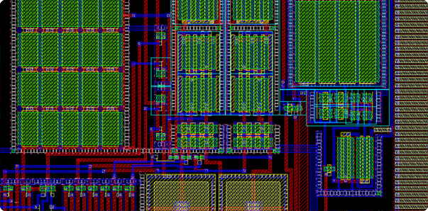
Physical Design, Signoff & PV
Expertise in place & route for block build/full chip development with
timing closure using industry-standard tools for tasks like Synthesis,
Floor Plan, Placement, CTS, Signal Integrity, IR Draw, EM, Low Power
Checks, and Signoff checks. Extensive Knowledge in physical
verification like DRC, LVS, Antenna, and Density in the latest nodes.
Having an in-depth knowledge and exposure in STA provides opportunity in exploring and understanding how other domains operate to design chip.
DFT scan insertion and Timing closure in Functional/Test modes.
Having an in-depth knowledge and exposure in STA provides opportunity in exploring and understanding how other domains operate to design chip.
DFT scan insertion and Timing closure in Functional/Test modes.
- ATPG
- FPGA-to-FPGA, FPGA-to-ASIC, ASIC-to-FPGA conversion
- Test pattern generation and simulation,Coverage improvement,IDDQ,BIST,BSCAN,DFT Spyglass checks


